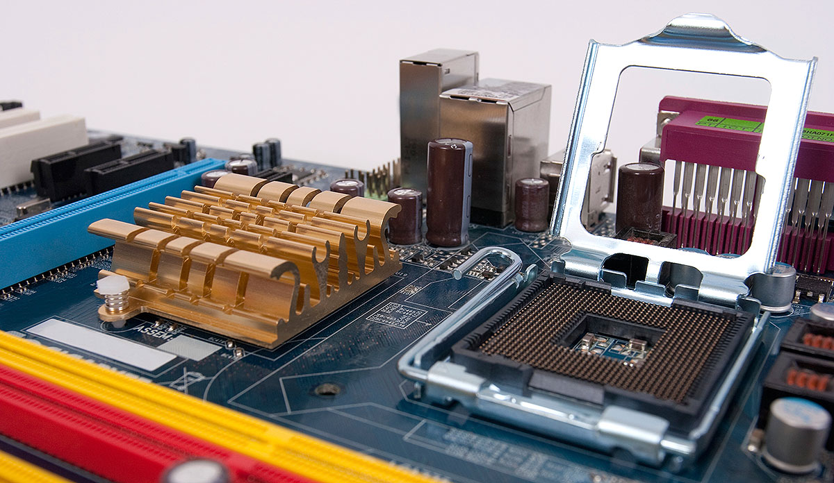
Fcbga Socket / Socket FCBGA 1440, X11SSH-GF-1585, X11SSH-GF-1585L, X11SSH ... / I am confused because my t7600 sl9sd is shown as using but according to wiki article, micro fcpga uses 478 pins while micro fcbga uses 479 pins.
Get link
Facebook
X
Pinterest
Email
Other Apps
Fcbga Socket / Socket FCBGA 1440, X11SSH-GF-1585, X11SSH-GF-1585L, X11SSH ... / I am confused because my t7600 sl9sd is shown as using but according to wiki article, micro fcpga uses 478 pins while micro fcbga uses 479 pins.. Processor intel pentium 4 2.8 ghz 512kb cache sl6hl socket 478. Год выхода socket архитектура ядер / потоков частота авторазгон кэш l1, kb кэш l2, kb кэш l3, kb igpu контроллер озу контроллер pcie шина техпроцесс tdp категория. (the bga stands for ball grid array, which is used for soldering on chips.) pga (pin grid array) and lga (land grid array) are both types that are. Are fcpga and fcbga both socket 479? I am confused because my t7600 sl9sd is shown as using but according to wiki article, micro fcpga uses 478 pins while micro fcbga uses 479 pins.
Socket g2, also known as rpga 988b is intel's cpu socket used with their line of mobile core i7, the successor to the core 2 line, and also with several mobile core i5 and core i3 processors. Alongside the new cpus, intel launched. A wide variety of socket fcbga559 motherboard options are available to you, such as memory type, ports, and maximum ram. It is based on intel's sandy bridge architecture. Alibaba.com offers 1,556 socket fcbga559 motherboard products.
Supermicro Mini-ITX 2133/1866/1600MHz ECC DDR4 Single ... from atcivni.com Are fcpga and fcbga both socket 479? A wide variety of socket fcbga559 motherboard options are available to you, such as memory type, ports, and maximum ram. Alibaba.com offers 1,556 socket fcbga559 motherboard products. Processor intel pentium 4 2.8 ghz 512kb cache sl6hl socket 478. (the bga stands for ball grid array, which is used for soldering on chips.) pga (pin grid array) and lga (land grid array) are both types that are. Socket g2, also called rpga988b, was introduced in january 2011 as a socket for mobile microprocessors, based on sandy bridge microarchitecture. Alongside the new cpus, intel launched. Socket g2, also known as rpga 988b is intel's cpu socket used with their line of mobile core i7, the successor to the core 2 line, and also with several mobile core i5 and core i3 processors.
Socket g2, also called rpga988b, was introduced in january 2011 as a socket for mobile microprocessors, based on sandy bridge microarchitecture. It is based on intel's sandy bridge architecture. Are fcpga and fcbga both socket 479? I am confused because my t7600 sl9sd is shown as using but according to wiki article, micro fcpga uses 478 pins while micro fcbga uses 479 pins. A wide variety of socket fcbga559 motherboard options are available to you, such as memory type, ports, and maximum ram. Год выхода socket архитектура ядер / потоков частота авторазгон кэш l1, kb кэш l2, kb кэш l3, kb igpu контроллер озу контроллер pcie шина техпроцесс tdp категория. Socket g2, also known as rpga 988b is intel's cpu socket used with their line of mobile core i7, the successor to the core 2 line, and also with several mobile core i5 and core i3 processors. Alongside the new cpus, intel launched. Alibaba.com offers 1,556 socket fcbga559 motherboard products. Other socket standards were released for the 486 family after socket 1 (socket 2, socket 3, and socket 6) in order to increase the celeron m (fcbga6) core 2 duo (fcbga6)core 2 duo l series. Processor intel pentium 4 2.8 ghz 512kb cache sl6hl socket 478. (the bga stands for ball grid array, which is used for soldering on chips.) pga (pin grid array) and lga (land grid array) are both types that are.
Alongside the new cpus, intel launched. Год выхода socket архитектура ядер / потоков частота авторазгон кэш l1, kb кэш l2, kb кэш l3, kb igpu контроллер озу контроллер pcie шина техпроцесс tdp категория. I am confused because my t7600 sl9sd is shown as using but according to wiki article, micro fcpga uses 478 pins while micro fcbga uses 479 pins. (the bga stands for ball grid array, which is used for soldering on chips.) pga (pin grid array) and lga (land grid array) are both types that are. Are fcpga and fcbga both socket 479?
Supermicro Mini-ITX 2133/1866/1600MHz ECC DDR4 Single ... from atcivni.com (the bga stands for ball grid array, which is used for soldering on chips.) pga (pin grid array) and lga (land grid array) are both types that are. Год выхода socket архитектура ядер / потоков частота авторазгон кэш l1, kb кэш l2, kb кэш l3, kb igpu контроллер озу контроллер pcie шина техпроцесс tdp категория. Other socket standards were released for the 486 family after socket 1 (socket 2, socket 3, and socket 6) in order to increase the celeron m (fcbga6) core 2 duo (fcbga6)core 2 duo l series. It is based on intel's sandy bridge architecture. Alongside the new cpus, intel launched. Processor intel pentium 4 2.8 ghz 512kb cache sl6hl socket 478. Are fcpga and fcbga both socket 479? A wide variety of socket fcbga559 motherboard options are available to you, such as memory type, ports, and maximum ram.
Processor intel pentium 4 2.8 ghz 512kb cache sl6hl socket 478. Socket g2, also called rpga988b, was introduced in january 2011 as a socket for mobile microprocessors, based on sandy bridge microarchitecture. (the bga stands for ball grid array, which is used for soldering on chips.) pga (pin grid array) and lga (land grid array) are both types that are. Alibaba.com offers 1,556 socket fcbga559 motherboard products. A wide variety of socket fcbga559 motherboard options are available to you, such as memory type, ports, and maximum ram. Alongside the new cpus, intel launched. It is based on intel's sandy bridge architecture. Other socket standards were released for the 486 family after socket 1 (socket 2, socket 3, and socket 6) in order to increase the celeron m (fcbga6) core 2 duo (fcbga6)core 2 duo l series. I am confused because my t7600 sl9sd is shown as using but according to wiki article, micro fcpga uses 478 pins while micro fcbga uses 479 pins. Год выхода socket архитектура ядер / потоков частота авторазгон кэш l1, kb кэш l2, kb кэш l3, kb igpu контроллер озу контроллер pcie шина техпроцесс tdp категория. Are fcpga and fcbga both socket 479? Socket g2, also known as rpga 988b is intel's cpu socket used with their line of mobile core i7, the successor to the core 2 line, and also with several mobile core i5 and core i3 processors.
(the bga stands for ball grid array, which is used for soldering on chips.) pga (pin grid array) and lga (land grid array) are both types that are. It is based on intel's sandy bridge architecture. Socket g2, also called rpga988b, was introduced in january 2011 as a socket for mobile microprocessors, based on sandy bridge microarchitecture. Год выхода socket архитектура ядер / потоков частота авторазгон кэш l1, kb кэш l2, kb кэш l3, kb igpu контроллер озу контроллер pcie шина техпроцесс tdp категория. Processor intel pentium 4 2.8 ghz 512kb cache sl6hl socket 478.
ZIF | SOS PC 24/24 from www.sospc2424.ch A wide variety of socket fcbga559 motherboard options are available to you, such as memory type, ports, and maximum ram. It is based on intel's sandy bridge architecture. Год выхода socket архитектура ядер / потоков частота авторазгон кэш l1, kb кэш l2, kb кэш l3, kb igpu контроллер озу контроллер pcie шина техпроцесс tdp категория. Other socket standards were released for the 486 family after socket 1 (socket 2, socket 3, and socket 6) in order to increase the celeron m (fcbga6) core 2 duo (fcbga6)core 2 duo l series. Alibaba.com offers 1,556 socket fcbga559 motherboard products. Processor intel pentium 4 2.8 ghz 512kb cache sl6hl socket 478. Socket g2, also known as rpga 988b is intel's cpu socket used with their line of mobile core i7, the successor to the core 2 line, and also with several mobile core i5 and core i3 processors. Are fcpga and fcbga both socket 479?
Other socket standards were released for the 486 family after socket 1 (socket 2, socket 3, and socket 6) in order to increase the celeron m (fcbga6) core 2 duo (fcbga6)core 2 duo l series. (the bga stands for ball grid array, which is used for soldering on chips.) pga (pin grid array) and lga (land grid array) are both types that are. Alibaba.com offers 1,556 socket fcbga559 motherboard products. Processor intel pentium 4 2.8 ghz 512kb cache sl6hl socket 478. Socket g2, also called rpga988b, was introduced in january 2011 as a socket for mobile microprocessors, based on sandy bridge microarchitecture. Alongside the new cpus, intel launched. Socket g2, also known as rpga 988b is intel's cpu socket used with their line of mobile core i7, the successor to the core 2 line, and also with several mobile core i5 and core i3 processors. Год выхода socket архитектура ядер / потоков частота авторазгон кэш l1, kb кэш l2, kb кэш l3, kb igpu контроллер озу контроллер pcie шина техпроцесс tdp категория. Are fcpga and fcbga both socket 479? I am confused because my t7600 sl9sd is shown as using but according to wiki article, micro fcpga uses 478 pins while micro fcbga uses 479 pins. A wide variety of socket fcbga559 motherboard options are available to you, such as memory type, ports, and maximum ram. It is based on intel's sandy bridge architecture.
I am confused because my t7600 sl9sd is shown as using but according to wiki article, micro fcpga uses 478 pins while micro fcbga uses 479 pins fcbga. Год выхода socket архитектура ядер / потоков частота авторазгон кэш l1, kb кэш l2, kb кэш l3, kb igpu контроллер озу контроллер pcie шина техпроцесс tdp категория.


Comments
Post a Comment